Friday, April 25, 2025
Wednesday, February 19, 2025
Thursday, August 17, 2023
Brian Cox Breaks Silence: "The Universe Existed Before Big Bang"
Modern Science explains the origin of the universe with the Big Bang Theory.
According to this theory, our world emerged from the explosion of singularity, a point in space-time where energy density and mass approach infinity, and all dimensions reach zero.
But Recently, Brian Cox has made a bold announcement stating that the universe has always existed and the Big Bang Theory is wrong.
Tuesday, June 20, 2023
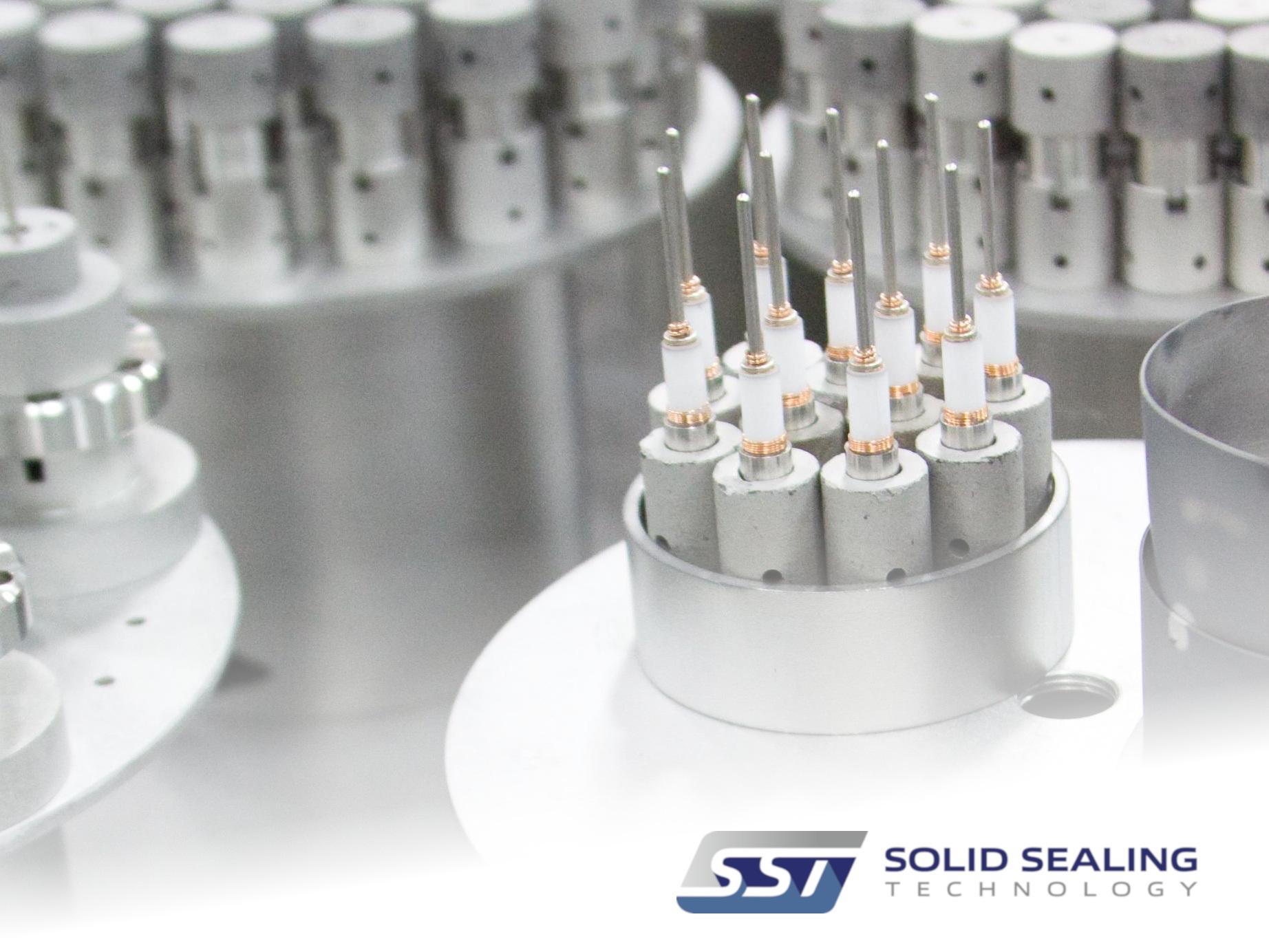
Welcome to Solid Sealing Technology
Solid Sealing Technology Capabilities.
Experts in hermetic feedthroughs and connectors.
Thursday, March 23, 2023
Custom Vacuum Designs
Over the years xtronix has delivered many custom designed products, both systems and components. xtronix custom designs removes the burdensome task of design engineering, parts procurement, assembly, testing and final qualification. We work with suppliers, often companies we actively distribute products of, to obtain the best price and delivery, leaving our customers more time to focus on their own applications and less time worrying about all the intricacies of custom designs. Solid Sealing Technology (SST) partners with us for various custom feedthrough assemblies. Here is an overview of their capabilities:


The basis of most Solid Sealing Technology products is ceramic-to-metal sealing and/or glass-ceramic sealing. The process of making your custom part(s) begins with a comprehensive review of engineering needs that ensures a complete understanding of the application’s requirements. A skilled team will define a production plan that gets you your hermetic feedthroughs and connectors quickly.
MATERIAL SOURCING
SST materials and components are sourced from world-class suppliers. Detailed documentation and specifications are available for all custom hermetic feedthroughs and connectors to ensure the materials meet your needs.
PRECISION CLEANING
All components at SST must meet strict standards and are processed through a customized cleaning system. The standardized process includes a specialty aqueous cleaner followed by a cascade DI water rinse. This cleaning process has been used and approved by key customers like Sandia National Labs and the United States' Army. The same process can be used for precision cleaning of metals, ceramics, and glass and is suitable for UHV environments. SST will ship your custom hermetic products sealed so they are ready to use out of the box.
MANUFACTURING
With your production plan in place, SST will begin manufacturing your parts. Whether you are creating a completely new custom hermetic product or modifying one of our many hermetic feedthroughs or connectors, we offer a technology suite that will meet your needs. SST offers metalizing and plating of ceramics, active metal joining, vacuum and hydrogen brazing, glass-ceramic sealing, TIG welding, spot welding, machining, and mechanical assembly.
FINAL INSPECTION & TESTING
SST verifies all critical requirements before shipping, and the customer service team will provide any product-related resources you need. SST offers vacuum-bagging and other special packaging options if needed. Parts will arrive clean and ready to use out of the box.
- Helium Leak Detection – 100% of SST parts are leak tested before shipping. Parts are tested to a leak rate of less than 1x10^-10 atm.cc/sec
- Pressure Testing - Hydrostatic Pressure testing up to 30,000 psi
- Electrical Testing – Continuity, HiPot/DWV (Dielectric Withstanding Voltage), Megohm Resistance, Capacitance, Heat Rise Testing
- Physical Testing - Torque, Push-Pull Testing, Engagement Force Measurement
- CMM, Vision Systems, Go/No-Go thread and pin gauges, Surface Profilometer, and certified metrology equipment for inspection and analysis
- XRF Thickness Testing of Coatings & Material Verification
- Basic Thermal Testing: LN2 exposure, vacuum bakeout
- Fiber Optic Insertion Loss Testing
Thursday, March 9, 2023
The most efficient Radionuclide Identifying Device (RID)
Detects and identifies nuclides in mixed, shielded and heavily masked configurations including Special Nuclear Material (SNM).
The DiscoveRAD is ultra-compact, rugged, sensitive, lightweight and.... is even game for a dip to 10 meters 1(IP68)!
Spectrometry at up to 1 million cps between 10 KeV to 1 MeV.


Wednesday, March 8, 2023
High Sensitivity Multifunction Compton Camera
|
Compton imaging exploits inelastic scattering, known as Compton scattering, using a Compton camera consisting of a scatterer detector in the front layer and an absorber detector in the back layer. Compton imaging can discriminate gamma rays over a wide energy range from several hundred keV to several MeV. Damavan Imaging was founded in 2014 to develop its 8 Temporal Imaging proprietary patents and software. In 2015 it won a big grant from the French Nuclear Waste Agency, ANDRA, to develop a Compton camera able to image low activity waste. In 2018 Damavan Imaging won a Horizon 2020 EU SME Award. Product Introduction: Temporal Imaging is a new concept for gamma ray imaging that uses both light and time distribution of each scintillation event to localize precisely each scintillation event in space (X,Y,Z), time (T) and energy (E). This new imaging concept allows an improvement on the voxel size for each scintillation event (1x1x2mm) on each of the two detector plates. It also allows a coincidence veto between the 2 Compton plates. Temporal δ Delta is the first device to use this new concept. It has an exceptional Signal/noise ratio thanks to the time veto between it’s 2 plates. The Temporal δ Delta V3 is equipped with a small spectroscopic CZT detector and also enable isotope identification, simple dosimetry and 4 Pi source detection. Temporal δ is the best Compton imager (400 KeV - 3000 KeV), excellent spectrometer (50 KeV - 3000 KeV), stable photon counter with dose estimation. |
Thursday, November 3, 2022
Selecting the best crystal for your coating process
A quartz crystal microbalance (QCM) takes advantage of the piezoelectric effect found in quartz crystals. Application of an electric potential across the quartz crystal induces mechanical shear strain in the crystal. If the polarity of this electric potential is reversed, the strain direction reverses. Rapid oscillation of the electric potential polarity leads to vibrational motion of the quartz crystal. Under the proper conditions, this vibration can induce an acoustic standing wave between the two crystal faces. The frequency of the standing wave is proportional to the thickness of the quartz crystal. If additional material is uniformly deposited on the face of the crystal, the additional thickness will decrease the resonant frequency of the acoustic wave. This frequency shift due to mass deposition may be correlated to the absolute mass deposited via the following substituted form of the Sauerbrey equation:

Tuesday, October 11, 2022
10 μm-thick four-quadrant transmissive silicon photodiodes for beam position monitor application: electrical characterization and gamma irradiation effects
Abstract:
Silicon photodiodes are very useful devices as X-ray beam monitors in synchrotron radiation beamlines. Owing to Si absorption, devices thinner than 10 µm are needed to achieve transmission over 90% for energies above 10 keV.
In this work, new segmented four-quadrant diodes for beam alignment purposes are fabricated on both ultrathin (10 µm-thick) and bulk silicon substrates. Four-quadrant diodes implementing different design parameters as well as auxiliary test structures (single diodes and MOS capacitors) are studied. An extensive electrical characterization, including current-voltage (I-V) and capacitance-voltage (C-V) techniques, is carried out on non-irradiated and gamma-irradiated devices up to 100 Mrad doses. Special attention is devoted to the study of radiation-induced charge build-up in diode interquadrant isolation dielectric, as well as its impact on device interquadrant resistance.
Finally, the devices have been characterized with an 8 keV laboratory X-ray source at 108 ph/s and in BL13-XALOC ALBA Synchrotron beamline with 1011 ph/s and energies from 6 to 16 keV. Sensitivity, spatial resolution and uniformity of the devices have been evaluated

Thursday, September 1, 2022
A1427 KIT Low Noise Fast Current Preamplifier & Discriminator


A1427 Kit configuration is also available. It includes the A1427 and the A1428 assembled together, both for fission chambers and for proton recoil detectors.
Features:
- Fast non-inverting preamplifier, negative output (EOUT)
- Input impedance: 50 Ω AC coupled
- Output high impedance (EOUT)
- Bipolar output high impedance (FOUT)
- Test input (TEST IN) impedance: 50 Ω, negative polarity
- FOUT/DET IN gain (FOUT negative lobe):
- FC version: 700÷2500
- PR version: 500÷1500
- FOUT/TEST IN gain: 1/100 of DET IN gain
- Output noise (peak to peak) < 40 mV
- Up to 3 kV detector bias voltage (HV IN)
- Rbias: 200 kΩ
Monday, February 21, 2022
WELCOME TO SOLID SEALING TECHNOLOGY
Wednesday, February 16, 2022
New Portable Device for Automated Radon Detection
The Spanish National Research Council (CSIC), through the Institute of Microelectronics of Barcelona (IMB-CNM-CSIC), has collaborated in the design and development of a prototype for the detection of radon gas, a naturally occurring radioactive gas that can be found in the interior spaces of buildings. It consists of a small device that connects to a wireless network and automatically monitors radon levels in its environment in buildings. This detection system contains a silicon sensor manufactured in the Clean Room of the IMB-CNM-CSIC.
The prototype, still in the standardization phase, is the result of the CARE project, an initiative that has been led by the company Alibava Systems and has had the participation of two public research centers, the IMB-CNM-CSIC and the Instituto Galego de Física de Altas Enerxías (IGFAE) of the Universidade de Santiago de Compostela, which has been responsible for carrying out the calibration and validation tests, both in its experimental facilities and in real environments. CARE also involves three companies, ATI Sistemas SL, Radiansa Consulting SL, Sensing & Control Systems SL.
Tuesday, October 5, 2021
Compact Tracking Telescope for High Energy Particles
OVERVIEW
The ALIBAVA Telescope has been successfully operated at the DESY and CERN-SPS beam lines.
The telescope consists of at least three planes (stations). The stations use ALIBAVA daughter boards to take the tracking information from two 90 degrees-turned strip sensors for XY positioning. The stations act as reference frame and allow precise track reconstruction. Each daughter connects to an ALIBAVA motherboard to process the information and they to a unique master board that synchronizes and controls the whole system. The system is triggered by two scintillators located at both ends.
Several devices can be tested simultaneously. Analysis of charge collection, cluster width, efficiency, resolution, time profile and other parameters of the devices under test with the software provided.
The telescope provides accurate particle tracking and hit point projection on device under test.
FEATURES
This product is sold under license of Spanish National Research Council (CSIC) and University of Valencia (Spain)
- Sensor: Microstrip Silicon, P‐on‐N silicon.
- Sensor size: 10x10 mm2
- Thickness: 300 μm
- Read-out channels: 128
- Pitch: 80 μm
- Spatial resolution: < 10 μm
- Chip BEETLE (technology from CERN/LHC)
- Clock speed: 40 MHz
- Dynamic range: 4 MIP
- Synchronous external trigger. Trigger boards available.
- Analysis software for Windows, Linux, Mac.
- Station dimensions: 100x80 mm2
- Mother and Master board dimensions: 247x172x32 mm3
- Voltage supply: +5 V
- Mechanical structure and cooling available
Wednesday, September 8, 2021
What is a Kelvin probe?

The Kelvin probe is a non-contact, non-destructive vibrating capacitor device used to measure the work function (wf) of conducting materials or surface potential (sp) of semiconductor or insulating surfaces. The wf of a surface is typically defined by the topmost 1 - 3 layers of atoms or molecules, so the Kelvin probe is one of the most sensitive surface analysis techniques available. KP Technology systems offer a very high wf resolution of 1 - 3 meV, currently the highest achieved by any commercial device.
The Kelvin probe does not actually touch the surface; rather an electrical contact is made to another part of the sample or sample holder. The probe tip is typically 0.2 - 2.0 mm away from the sample and it measures the 'traditional work function', i.e. that found in literature tables. Other techniques, using very sharp tips some 10's of nanometers away from the sample, measure very reduced and distorted work functions due to the close separation of tip and sample.
Tuesday, September 7, 2021
Hands-on Educational Tool for Physics
Thursday, June 10, 2021
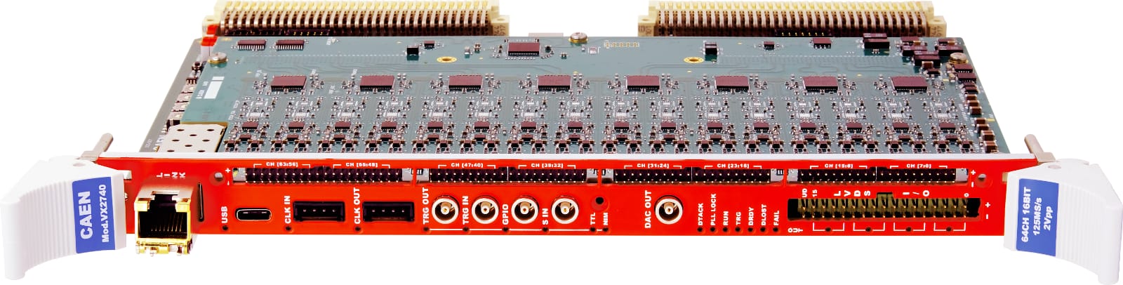
CAEN Digitizer Whitepaper
- More density, faster sampling rate, higher resolution for higher performances
- Increased communication readout through 1/10 Gb Ethernet, USB 3.0 (yet keeping proprietary CONET)
- Easier multi-board synchronization (clock and timing distribution)
- Increase of acquisition memory buffer size: from SSRAM to DDR4 (=> from MBs to GBs)
- Single FPGA (Xilinx Zynq US+ ) architecture => more resources for DPP algorithms and support for “Open FPGA”
- Embedded quad-core ARM (Linux) => middleware, web interface. Possibility to run user Data Processing SW
Friday, January 22, 2021
CAEN x1081 Programmable Logic Units
Coincidence, Trigger Logic, Counter, Pulse Generator and more

>>> Click to start video <<<