Showing posts with label Thin Films. Show all posts

Tuesday, June 20, 2023

Thursday, March 23, 2023

Custom Vacuum Designs

Over the years xtronix has delivered many custom designed products, both systems and components. xtronix custom designs removes the burdensome task of design engineering, parts procurement, assembly, testing and final qualification. We work with suppliers, often companies we actively distribute products of, to obtain the best price and delivery, leaving our customers more time to focus on their own applications and less time worrying about all the intricacies of custom designs. Solid Sealing Technology (SST) partners with us for various custom feedthrough assemblies. Here is an overview of their capabilities:

DESIGN REVIEW
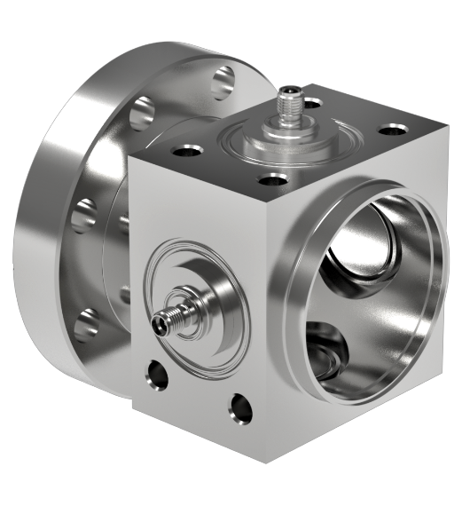
The basis of most Solid Sealing Technology products is ceramic-to-metal sealing and/or glass-ceramic sealing. The process of making your custom part(s) begins with a comprehensive review of engineering needs that ensures a complete understanding of the application’s requirements. A skilled team will define a production plan that gets you your hermetic feedthroughs and connectors quickly. 

MATERIAL SOURCING
SST materials and components are sourced from world-class suppliers. Detailed documentation and specifications are available for all custom hermetic feedthroughs and connectors to ensure the materials meet your needs. 

PRECISION CLEANING
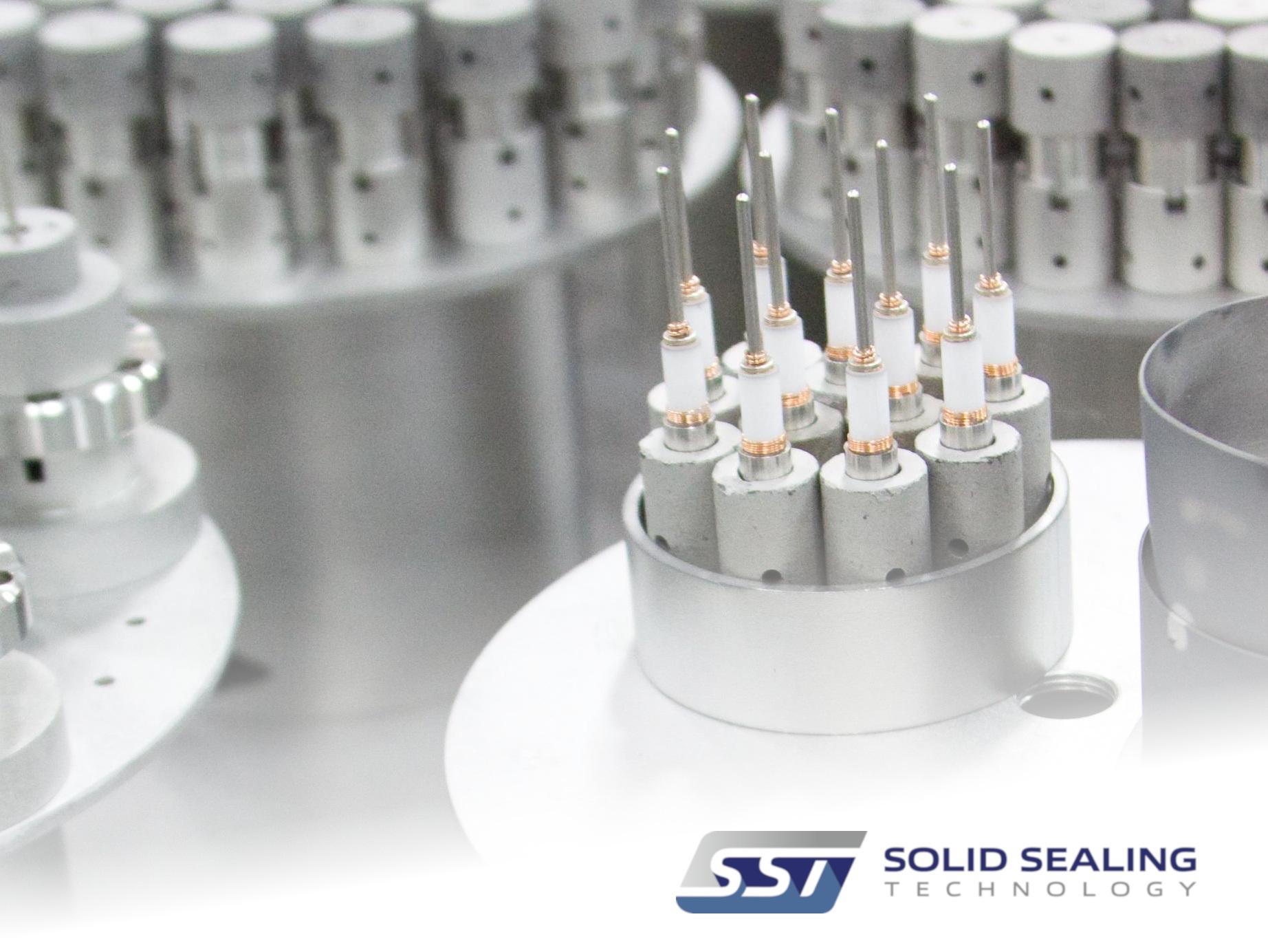
All components at SST must meet strict standards and are processed through a customized cleaning system. The standardized process includes a specialty aqueous cleaner followed by a cascade DI water rinse. This cleaning process has been used and approved by key customers like Sandia National Labs and the United States' Army. The same process can be used for precision cleaning of metals, ceramics, and glass and is suitable for UHV environments. SST will ship your custom hermetic products sealed so they are ready to use out of the box. 

MANUFACTURING
With your production plan in place, SST will begin manufacturing your parts. Whether you are creating a completely new custom hermetic product or modifying one of our many hermetic feedthroughs or connectors, we offer a technology suite that will meet your needs. SST offers metalizing and plating of ceramics, active metal joining, vacuum and hydrogen brazing, glass-ceramic sealing, TIG welding, spot welding, machining, and mechanical assembly. 

FINAL INSPECTION & TESTING
SST verifies all critical requirements before shipping, and the customer service team will provide any product-related resources you need. SST offers vacuum-bagging and other special packaging options if needed. Parts will arrive clean and ready to use out of the box.

Calibrated tools, vision systems, and a CMM are used to verify mechanical attributes. And electrical requirements are validated with the latest electrical test equipment. SST is certified compliant to ISO9001:2015 and often works within the more stringent requirements of defense and medical customers.
  • Helium Leak Detection – 100% of SST parts are leak tested before shipping. Parts are tested to a leak rate of less than 1x10^-10 atm.cc/sec
  • Pressure Testing - Hydrostatic Pressure testing up to 30,000 psi
  • Electrical Testing – Continuity, HiPot/DWV (Dielectric Withstanding Voltage), Megohm Resistance, Capacitance, Heat Rise Testing
  • Physical Testing - Torque, Push-Pull Testing, Engagement Force Measurement
  • CMM, Vision Systems, Go/No-Go thread and pin gauges, Surface Profilometer, and certified metrology equipment for inspection and analysis
  • XRF Thickness Testing of Coatings & Material Verification
  • Basic Thermal Testing: LN2 exposure, vacuum bakeout
  • Fiber Optic Insertion Loss Testing

Click for more

Thursday, November 3, 2022

Selecting the best crystal for your coating process

A quartz crystal microbalance (QCM) takes advantage of the piezoelectric effect found in quartz crystals. Application of an electric potential across the quartz crystal induces mechanical shear strain in the crystal. If the polarity of this electric potential is reversed, the strain direction reverses. Rapid oscillation of the electric potential polarity leads to vibrational motion of the quartz crystal. Under the proper conditions, this vibration can induce an acoustic standing wave between the two crystal faces. The frequency of the standing wave is proportional to the thickness of the quartz crystal. If additional material is uniformly deposited on the face of the crystal, the additional thickness will decrease the resonant frequency of the acoustic wave. This frequency shift due to mass deposition may be correlated to the absolute mass deposited via the following substituted form of the Sauerbrey equation:

where pq is the density of quartz, Aq is the area of resonance, Nq is a frequency constant for AT-cut quartz crystals (1.668 X 10⁵ Hz cm), Fq is the frequency of quartz prior to deposition, and F is the frequency at any point during the deposition process. This equation is only valid if the total frequency shift is kept within 2% of the starting frequency. 

In summary, the thickness of the added layer changes the wavelength of the standing wave resonance. In essence, a deposited film acts as if the quartz is increasing in thickness. The thicker the crystal, the longer the resonance wavelength. This is measured as a frequency shift at the monitor. The film density value is input in order to compensate the density difference between the film deposited and the density of quartz which is 2.648 g/cc.

Monday, February 21, 2022

WELCOME TO SOLID SEALING TECHNOLOGY

Solid Sealing Technology (SST) designs and manufactures essential electrical components for today’s high-tech world. SST's innovative material-joining technologies bond ceramics and glass to metal to create hermetic feedthroughs and connectors tailored for use in vacuum environments. Experts in design, SST offers a vast catalog of standard high-performance sealing solutions that improve reliability in demanding engineering settings. And for customers with unique challenges, SST’s skilled engineering group creates fully customized parts from the ground up. Working with an unrivaled commitment to quality and customer service, SST inspires innovation and enables technology around the world.

With a focus on customer satisfaction, SST strives to constantly improve their quality management system and product performance. SST are proud to be ISO9001 certified. 

Solid Sealing Technology's commitment to continuous improvement extends to all aspects of their business, from the first contact with customers to delivery of your final part. Through persistent attention to quality and customer service, SST ensure that they meet customers' needs with reliable high-performing vacuum products spanning feedthroughs, connectors, isolators, viewports, pinch-off tubes, and related accessories for both air-side and vacuum-side use.
SST engineers work closely with every customer to deliver custom hermetic solutions that can be found behind the scenes of some of the world’s most advanced technologies. Examples include industrial, medical, and research facilities where SST parts are used in equipment like energy storage systems, MRI machines, and particle accelerators. They have even sent parts to Mars, empowering NASA’s Mars Insight Mission to tackle the challenges of our solar system. Highly InnovativeCreatively Bespoke, and Impressively Robust, SST hermetic sealing solutions help push the boundaries of technological advancement in an evolving world.

Tuesday, January 5, 2021

Solid Sealing Technology Starts 2021 With New Website

Solid Sealing Technology, our partners in Ceramic Feedthroughs and thousands of industry standard parts for vacuum technology, have opened 2021 with a new website which we invite you to visit: www.solidsealing.com 

Solid Sealing Technology designs and manufactures essential electrical components for today’s high-tech world. Their innovative material-joining technologies bond ceramics and glass to metal to create hermetic feedthroughs and connectors tailored for use in vacuum environments. Experts in design, SST offers a vast catalog of standard high-performance sealing solutions that improve reliability in demanding engineering settings. And for customers with unique challenges, SST’s skilled engineering group creates fully customized parts from the ground up.

SST products include: vacuum feedthroughs, hermetic connectors, ceramic-to-metal sealing, metalizing and brazing of ceramics, glass-ceramic sealing, sapphire viewports, UHV-grade copper pinch-off tubules and custom feedthrough design.


SST engineers work closely with every customer to deliver custom hermetic solutions and industry-leading ceramic-to-metal seals that can be found behind the scenes of some of the world’s most advanced technologies. Examples include industrial, medical, and research facilities where SST parts are used in equipment like energy storage systems, MRI machines, and particle accelerators. SST have even sent parts to Mars, empowering NASA’s Mars Insight Mission to tackle the challenges of our solar system. Highly Innovative, Creatively Bespoke, and Impressively Robust, SST vacuum feedthroughs and hermetic connectors help push the boundaries of technological advancement in an evolving world.


Thursday, September 14, 2017

Simplified fabrication process for high-efficiency solar cells

A team of EPFL and CSEM researchers in Neuchâtel presents in Nature Energy a new astonishing method of creating crystalline solar cells with electrical contacts at the rear, suppressing all shadowing at the front. Thanks to the new inexpensive approach, the fabrication process is strongly simplified with efficiencies in the laboratory already surpassing 23%.

In the quest for more efficient crystalline silicon solar cells with low manufacturing costs, one of the most promising approach is to bring all electrical contacts at the back of the device. This suppresses all shadowing at the front, increasing the current and the efficiency. This approach generally requires several delicate processing steps, because well-defined narrow negative and positive contact lines need to be created, which will then collect the electrons (negative charges) and holes (positive charges). This requires usually several steps of masking of photolithography to create the alternated positive (+) and negative (-) areas.

 
Click for full details

Saturday, March 26, 2016

Simple and Fast Cryocooling for Thin Films

Using the CryoLab S or CryoLab MSG you can perform various types of measurements on your thin film sample including:
  1. - Critical temperature characterisation
  2. - Van der Pauw measurements
  3. - Seebeck coefficient
  4. - Thermal properties and many more
Using The CryoLab, it is possible to characterise your thin film from 373 Kelvin down to cryogenic temperatures.


Monday, February 1, 2016

The Future of Thin Film Control

http://www.xtronix.ch/qcm.htm

Eon-ID™ is a new film thickness controller that packages an ultra-high resolution deposition control system into a compact, rack-mountable enclosure.

Featuring integrated display, intuitive GUI, and durable architecture, Eon-ID™ offers an all-inclusive design that adapts easily to a variety of settings – ranging from industrial to laboratory to clean room to research environments. Eon-ID™ integrates well into existing rack thin film systems.

Monday, December 7, 2015

ORNL process could be white lightning to electronics industry

OAK RIDGE, Tenn., Dec. 1, 2015 – A new era of electronics and even quantum devices could be ushered in with the fabrication of a virtually perfect single layer of “white graphene,” according to researchers at the Department of Energy’s Oak Ridge National Laboratory.
 
The material, technically known as hexagonal boron nitride, features better transparency than its sister, graphene, is chemically inert, or non-reactive, and atomically smooth. It also features high mechanical strength and thermal conductivity. Unlike graphene, however, it is an insulator instead of a conductor of electricity, making it useful as a substrate and the foundation for the electronics in cell phones, laptops, tablets and many other devices.
 
“Imagine batteries, capacitors, solar cells, video screens and fuel cells as thin as a piece of paper,” said ORNL’s Yijing Stehle, postdoctoral associate and lead author of a paper published in Chemistry of Materials. She and colleagues are also working on a graphene hexagonal boron 2-D capacitor and fuel cell prototype that are not only “super thin” but also transparent.
 
With their recipe for white graphene, ORNL researchers hope to unleash the full potential of graphene, which has not delivered performance consistent with its theoretical value. With white graphene as a substrate, researchers believe they can help solve the problem while further reducing the thickness and increasing the flexibility of electronic devices.
 

Wednesday, June 24, 2015

Applications for the CryoLab cryocooler

Measurements at cryogenic temperatures were never this easy!

We recently launched a new line of plug-n-play desktop cryocoolers for applications requiring cooling of small samples to 90 K or further down to 75 K (i.e. SQUIDs).


http://www.xtronix.ch/cryolab.htm

 
Known as CryoLab, by Kryoz Technologies of Holland, the LN2-free low-temperature analysis cooling systems allow for  characterisation measurements from room temperature down to cryogenics in a fully automated manner. Doing measurements doesn’t require any experience or know-how on cryogenics, vacuum technology or thermodynamics from the user.

 
 http://www.xtronix.ch/cryolab.htm


Wednesday, November 5, 2014

A multi-detector, digitizer based neutron depth profiling device for characterizing thin film materials

P. L. Mulligan, L. R. Cao,a) and D. Turkoglu 

Nuclear Engineering Program, Department of Mechanical and Aerospace Engineering, The Ohio State University, Columbus, Ohio 43210, USA
 
Abstract
Neutron depth profiling (NDP) is a mature, nondestructive technique used to characterize the concentration of certain light isotopes in a material as a function of depth by measuring the residual energy of charged particles in neutron induced reactions. Historically, NDP has been performed using a single detector, resulting in low intrinsic detection efficiency, and limiting the technique largely to high flux research reactors. In this work, we describe a new NDP instrument design with higher detection efficiency by way of spectrum summing across multiple detectors. Such a design is capable of acquiring a statistically significant charged particle spectrum at facilities limited in neutron flux and operation time.
 
Click to view complete article
 

Friday, March 21, 2014

Next Generation Crystal Microbalances for Thin Film Deposition Monitoring & Control

by Scott Grimshaw, Colnatec USA

The "Achilles heel" of thin film deposition process monitoring and control is the quartz crystal microbalance (QCM). Since its advent in the 1960's, QCM's have been an integral part of most commercial thin film coating systems. Unfortunately, the limitations of QCM's for processes such as optical coating, ion beam sputtering, MBE and CVD have not been adequately addressed.
 
A new class of QCM sensor, designed for elevated temperatures, high stress dielectrics and extremely thin coatings is now available. This new sensor embodies an advanced crystallographic cut, "smart" sensor housings with integrated heaters, and novel crystal materials to extend the range of thin film monitoring to up to 250°C. 

INTRODUCTION
Quartz crystal microbalances operate in a relatively simple fashion. The QCM consists of a disc of quartz cut at a specific angle and shape from a bar of synthetically grown quartz. This quartz disc is then coupled into an electrical circuit and caused to vibrate at its natural resonance frequency. The resonance changes (decreases in frequency) whenever a thin film coating collects on the crystal surface. If the density of the film material is known, an algorithm can be used to compute the film thickness. 

Wednesday, January 29, 2014

Wafer-scale design of lightweight and transparent electronics that wraps around hairs

ETH Zürich contributors: Giovanni A. Salvatore, Niko Münzenrieder, Thomas Kinkeldei, Luisa Petti, Christoph Zysset, Ivo Strebel, Lars Büthe & Gerhard Tröster
A new way of making ultra thin, flexible and transparent electronics has been unveiled by researchers in Switzerland. The technique involves fabricating micron-thick electronic devices on a conventional silicon wafer, which is later detached by soaking it in water. The free-floating devices can then be placed onto a variety of biological tissues, including human skin and even a single hair. The technology could be used to make "smart" contact lenses for monitoring the pressure in an eyeball or for creating flexible solar cells.

Subscribe to eNewsTronix